|
* TinkerDifferent *
Retro Computing Community |
| Home | Forums | What's New | Search | Settings |
| WarpSE: 25 MHz 68HC000-based accelerator for Mac SE |
|
alxlab Active Tinkerer -------- Joined: Sep 23, 2021 Posts: 293 Likes: 323 |
Jan 10, 2022 - #21
This is really exciting :) Really looking forward to possibly trying it out when ever it's ready to test.
Liked by Zane Kaminski |
|
rjkucia Tinkerer Madison, Wisconsin, USA -------- Joined: Dec 21, 2021 Posts: 233 Likes: 81 |
Jan 10, 2022 - #22
Very cool! Do you have a target price in mind for this?
|
|
Zane Kaminski Administrator Columbus, Ohio, USA -------- Joined: Sep 5, 2021 Posts: 372 Likes: 615 |
Jan 11, 2022 - #23
Liked by rjkucia |
|
rjkucia Tinkerer Madison, Wisconsin, USA -------- Joined: Dec 21, 2021 Posts: 233 Likes: 81 |
Jan 11, 2022 - #24
I'm excited about it! A few questions (sorry if I missed them earlier in the thread):
-Is this designed as a plug-and-play deal? Or is there extra configuration/soldering/board work that would need to be done? -The 68HC000 is just a plain 68k clone right? Which means no built-in FPU, 32-bit compatibility, or MMU correct? -Would the replacement ROM enable 800k SEs to use Superdrives/HD floppy drives? Or is that still run through the onboard ROM? |
|
alxlab Active Tinkerer -------- Joined: Sep 23, 2021 Posts: 293 Likes: 323 |
Jan 11, 2022 - #25
The 68HC000 is a different model. It's actually used in the Macintosh Portable. No FPU or MMU. It has the same 32-bit capabilities as the original 68000. Here's the description from the MC68000 reference manual: "The primary benefit of the MC68HC000 is reduced power consumption. The device dissipates an order of magnitude less power than the HMOS MC68000. The MC68HC000 is an implementation of the M68000 16/-32 bit microprocessor architecture. The MC68HC000 has a 16-bit data bus implementation of the MC68000 and is upward code-compatible with the MC68010 virtual extensions and the MC68020 32-bit implementation of the architecture."
This would not convert an 800k SE to use Superdrives/HD floppy drives. This would require the Superdrives/HD floppy drive SWIM chip as well which still hasn't been re-implemented even though documentation is floating around. Liked by Zane Kaminskiandrjkucia |
|
Zane Kaminski Administrator Columbus, Ohio, USA -------- Joined: Sep 5, 2021 Posts: 372 Likes: 615 |
Jan 12, 2022 - #26
Yep, alxlab has it exactly right. You need the SWIM floppy chip (as opposed to IWM) on your SE motherboard in order to use 1.44 MB disks. Regarding the choice of CPU, MC68HC000 doesn't really offer any more features than MC68000, just lower power and more speed. There's also MC68SEC000 which is a newer revision that overclocks even better than MC68HC000 but this design doesn't use the 'SEC000. The final die shrink of the 'SEC000 is known to usually work at 50 MHz despite only being rated for 20 MHz. Of course the original 4 MB RAM limit still applies since the MC68HC000 doesn't have an MMU that it can use to move the peripheral I/O devices around and address more RAM. And it's completely plug-and-play of course. No need for any modifications to your SE board except for installing the card.
Liked by rjkucia |
|
Zane Kaminski Administrator Columbus, Ohio, USA -------- Joined: Sep 5, 2021 Posts: 372 Likes: 615 |
Jan 16, 2022 - #27
Update on the update system redesign (haha):
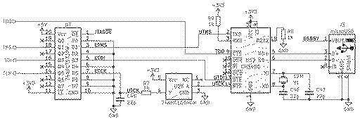
In the top left is the basic component placement for the new update system. It consists of the CH340G USB-serial chip, crystal (different, cheaper package than before), and just a single $0.15 74AHCT573 tristate buffer (really a latch but that functionality is unused). No more $3+ update microcontroller. When the USB is plugged in, the Mac is put into reset and buffer drives some bitbang signals from the CH340G onto the JTAG lines. Now for this arrangement we are basically abusing the RTS/CTS "modem control" signals to function as bitbang I/O. Upside is lower cost but the downside is that the bits can only be toggled at the USB polling rate of 1 kHz and multiple bits must be toggled to do one JTAG cycle. The bitstream for this CPLD is like 100 kilobits so it may take 10+ minutes to update the CPLD... I will make sure to put a progress bar... To be more specific, here is the update circuitry part of the schematic: So we have the USB port (on the right) and that goes to the CH340G USB-serial chip. Then it gets weird. We have the serial TXD pin connected to JTAG TMS, DTR connected to JTAG TDI, and serial RTS inverted by the '1G04 and then connected to JTAG TCK. JTAG TDO (output from the CPLD) is connected to serial CTS. The idea here is that we can toggle DTR, RTS, and TXD on the attached PC and thus update the FPGA over JTAG. DTR and RTS can be toggled rather explicitly. The trick to bringing TXD low indefinitely (as opposed to for just one character) is to assert a "break" condition. All of this bit twiddling can be accomplished via the Windows API for serial port extended functions, EscapeCommFunction(...): There is a similar windows API call, GetCommModemStatus(...) which can be used to read the CTS pin. With this Windows API, it will be easy to implement the pulse_tck function that accomplishes all of the bitbanging required to port libxsvf which will "play" the update XSVF file onto the CPLD in order to update it: So with all this I can estimate the time required to execute pulse_tck once and begin to estimate the total time required to do an update. The USB polling rate is 1ms so it takes 1ms to toggle TMS (if necessary), 1ms to toggle TDI (if necessary), 1ms to bring TCK low, and 1ms to bring it high. So to send a bit it takes 2ms if TMS and TDI don't need to change, otherwise 3 or 4ms. Usually when loading the bitstream, TMS will be 0... right? I think so but I can't quite remember the JTAG protocol. So hopefully if the toggle rate is 50% between bits it will be 2.5ms to send one bit. But then we have to poll TDO, so it may be another millisecond. So 3.5 milliseconds per bit? or 285 bits per second... Well the good news is that I think the XC95144XL has under 100,000 flash fuses so hopefully we will only have to run pulse_tck 100,000 times... right? And so that would amount to just under 6 minutes. But maybe we have to run pulse_tck two or three times per bit in the bitstream... so more like 12 or 18 minutes. Is this too long? Updates oughta be infrequent, just for bug fixes. Another thought is what operating systems to support. Is it a bad idea to make the update program just for Windows? I could do macOS too I guess but it seems like a bit of a waste of time compared to moving on to another project. Liked by rjkuciaandKai Robinson |
|
rjkucia Tinkerer Madison, Wisconsin, USA -------- Joined: Dec 21, 2021 Posts: 233 Likes: 81 |
Jan 16, 2022 - #28
Wow, I had no idea just getting USB to work was that involved on this thing!
I personally would be fine with just Windows, but as a second platform Linux would be my second vote. My only general concern would be if you based this around that one Windows API too closely which could lock out other platforms, or get deprecated and put us in a bad spot in the future. Windows is great at backwards compatibility but considering this is a device for a 35 year old computer, who knows what platforms will look like decades from now. |
|
Zane Kaminski Administrator Columbus, Ohio, USA -------- Joined: Sep 5, 2021 Posts: 372 Likes: 615 |
Jan 20, 2022 - #29
I finished my draft of the update program and it seems pretty good. It plays an XSVF file onto the CPLD's JTAG port using libxsvf. Now the sort of mediocre part is that the update speed is about 500 bits per second and the size of the overall update is more than 100,000 bits so it may take like 10 minutes.
Here's a screenshot of it "working," at least as well as it can without me having hardware in hand. I've got the PC connected to a CH340G USB chip I have on another board. The program doesn't do anything because there's no FPGA connected to the USB chip but I have confirmed that the bits are being twiddled as expected .
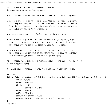
Soon it will be time to make prototypes! Edit: Here's the source for the update program if anyone is interested: https://github.com/garrettsworkshop/CH340G-XSVF
Liked by Patrick,alxlab,ericand 1 other person |
|
Zane Kaminski Administrator Columbus, Ohio, USA -------- Joined: Sep 5, 2021 Posts: 372 Likes: 615 |
Feb 14, 2022 - #30
Since a month ago I have slightly revised the update system so that now we can hopefully achieve 1 kbit/sec, double the previous rate. The change is basically to use the TXD pin of the serial port to send out the clock. I can send a character that has an on-the-wire representation that's a single low-going pulse. That will accomplish clocking the JTAG port. This doubles the speed since we just have to send the clock pulse character once rather than having to bring the clock low, wait, and then bring it back high.
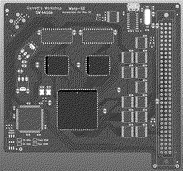
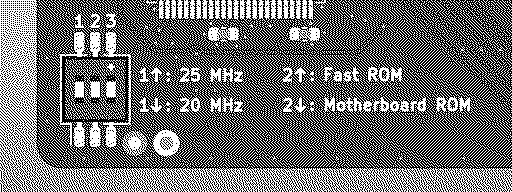
One thing I also need to know is whether the SE FDHD ROM works in an SE that doesn't have the the SWIM chip, just an IWM. Does this work? Does the floppy drive work in this case? Kai says he thinks it doesn't work and the FDHD ROM must be paired with the SWIM, not the IWM. That would be rather unfortunate since then I would have to basically halve the effective size of the onboard ROM to to store the FDHD and non-FDHD ROMs together. It'd be great if anyone could share any first-hand knowledge about whether you can use the FDHD ROM without a SWIM. Nevertheless I have decided (for unrelated component sourcing reasons) to switch to a triple DIP switch so there's an extra spot on the switch which we can use to toggle 800k/FDHD ROM. On that subject, is the DIP switch "legend" clear enough? My intent with this is to say that the left switch changes between 20/25 MHz, the middle one selects whether onboard or motherboard ROM is used, and then there's nothing for the right switch. Is this any good? It seems a little unclear, especially the lack of anything about the right switch, but I dunno how to make it better. Prototypes will be made once I get some Commodore 64 REU clone boards back from JLC, on which I am prototyping the update system. (I will post about that thing soon.) Once I verify correct operation of the update system on there I will fabbing some "Warp SE" prototypes. New schematic for the update system: [Image: UpdateSystem.png]
Liked by alxlab,Kai Robinsonandrjkucia |
|
rjkucia Tinkerer Madison, Wisconsin, USA -------- Joined: Dec 21, 2021 Posts: 233 Likes: 81 |
Feb 14, 2022 - #31
Do you intend to have the 3rd switch do something eventually? Or is it the type of deal where 3 switches is cheaper than 2, or something like that? Either way, I think it might be best to have a clear label/ID for the switch as a whole, and just have the detailed settings listed in documentation. |
|
Zane Kaminski Administrator Columbus, Ohio, USA -------- Joined: Sep 5, 2021 Posts: 372 Likes: 615 |
Feb 18, 2022 - #32
Yeah, I should probably go over it in the manual but I think it would be good to have some minimal description on the board if it's not too verbose or confusing. That way you won't have to refer to the manual to just make a quick change to the settings. As for the third switch, it's "insurance" in the sense that I might need to add another option later in development. So my current plans have it not doing anything but there's a fair likelihood that we will want a dip switch to do something in the future.
Is this any clearer?
Liked by wottle |
|
rjkucia Tinkerer Madison, Wisconsin, USA -------- Joined: Dec 21, 2021 Posts: 233 Likes: 81 |
Feb 18, 2022 - #33
Yeah I think that's perfect! The main issue with the other version was mentally figuring out exactly where the dots were, and this completely solves that!
Liked by Zane Kaminski |
|
Ubik Tinkerer Orange County, CA -------- Joined: Nov 2, 2021 Posts: 63 Likes: 81 |
Feb 19, 2022 - #34
I just want to add my support and that I will be happy to be a paying customer of this project. My SE works so wonderful with the SuperMac Speed Card 16Mhz 68000, so I agree the 68K is the way to go for compatibility. I would add it would be nice to solve the distorted sound issue that is prevalent with all SE accelerators.
Liked by Zane Kaminski |
|
Zane Kaminski Administrator Columbus, Ohio, USA -------- Joined: Sep 5, 2021 Posts: 372 Likes: 615 |
Mar 2, 2022 - #35
Okay! I have mostly confirmed proper operation of the update system on the unrelated Commodore 64 gizmo:
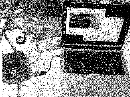
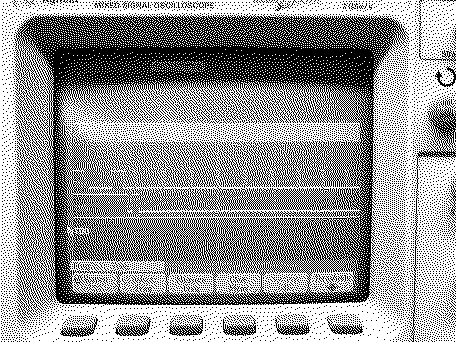
Here I've got the unrelated Commodore 64 gizmo hooked up to my MacBook which is running the update software in emulated Windows 7: Above this on the shelf I have an oscilloscope which is showing the JTAG signals: Only issue is that the data rate is not so good with emulated Windows 7 running on my ARM MacBook. Referring to the scope, the data rate is only 70 bits per second... This really slow speed is just an artifact of the emulator. On real x86/x64 hardware it will do the still pretty slow speed of 1 kbit/sec. Unfortunately there is no ARM driver for the CH340G USB-serial chip so I can't run the program in a Windows 11 VM on the MacBook. That would probably be a lot faster than QEMU if it was possible. Tomorrow I will be trying it on a real Windows 10 PC. I'd do it tonight but I accidentally broke the USB port off the board. Oops! Trying it on a "full-speed" computer is important to make sure there is sufficient setup and hold time for the TDI and TMS data signals relative to the TCK clock signal. Once I do that and actually update the CPLD on the unrelated Commodore gizmo I'll fab some prototypes of the Warp-SE!
Liked by Ubik,Kai Robinsonanderic |
|
Zane Kaminski Administrator Columbus, Ohio, USA -------- Joined: Sep 5, 2021 Posts: 372 Likes: 615 |
Mar 5, 2022 - #36
I have succeeded in making the update program recognize the chip on the unrelated commodore gizmo and reflash it!
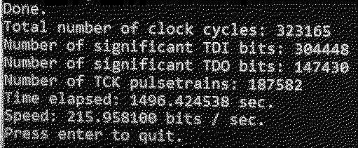
Here's a shot of the output of the update program recognizing the FPGA: And the update completes as expected: :) So it took 8 minutes and 40 seconds at a speed of 380 bits per second. Not bad! This is for the unrelated C64 gizmo but the update speed and size should be similar on the Warp-SE. That's just for programing and not verifying. With verification enabled it took much longer... 28 minutes. Readback of the data is just very slow, more like 125 bits per second instead of 380. Oh well, good enough. I'll try to make it faster in the future. Now it's time to make Warp-SE prototypes!
Liked by Ubik |
|
Zane Kaminski Administrator Columbus, Ohio, USA -------- Joined: Sep 5, 2021 Posts: 372 Likes: 615 |
Mar 6, 2022 - #37
Better update speeds! For programming only, not verifying, it takes only 3 minutes and 48 seconds:
Verifying is still the same speed, 21 minutes, so the total to program and verify is like 25 minutes: Okay enough with the update system. Booooringggg! But very useful of course. My next post oughta be about the final prototype board design which I will be sending to fab soon.
Liked by eric |
|
Patrick Tinkerer -------- Joined: Oct 26, 2021 Posts: 435 Likes: 226 |
Mar 11, 2022 - #38
well i for one will want to get in on the first batch.
Liked by UbikandZane Kaminski |
|
rjkucia Tinkerer Madison, Wisconsin, USA -------- Joined: Dec 21, 2021 Posts: 233 Likes: 81 |
Mar 11, 2022 - #39
Any estimate for how this will end up performing? At 25MHz & with the other improvements you've talked about it sounds like it would be a good deal faster than an SE/30, just without the extra memory capacity. Is that accurate?
|
|
Patrick Tinkerer -------- Joined: Oct 26, 2021 Posts: 435 Likes: 226 |
Mar 11, 2022 - #40
i'm curious about this answer as well.
my understanding is maybe it wouldn't because an '030 is also faster per cycle. that is. gets more done in a single cycle then a plain 68k ? that is . a 25Mhz 68000 is slower then a 25mhz 68030 that is. thats my guess. |
| << First | < Prev | Page 2 of 40 | Next > | Last >> |
| Home | Forums | What's New | Search | Bookmarks | RSS | Original | Settings |
| XenForo Retro Proxy by TinkerDifferent.com |
![[Image: UpdateSystem.png]](/proxy_image?url=https://tinkerdifferent.com/data/attachments/3/3106-285553e538e57dc5dd532f901c79908b.jpg)